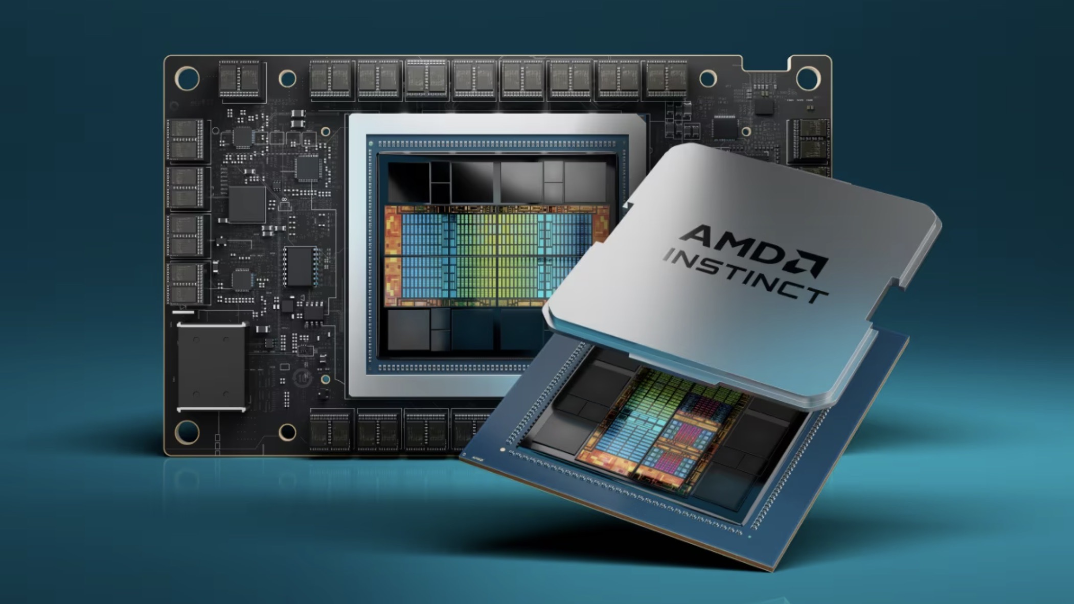
AMD has unveiled its latest accelerated processing unit (APU) built on the Zen 4 architecture in the form of the MI300A – which is expected to give Nvidia a run for its money as organizations flock to buy up components to power AI workloads.
The unit – the first APU for data centers, AI, and high-performance computing (HPC) workloads – comprises 24 threaded CPU cores alongside 228 CDNA 3 compute units that make up the GPU element.
The APU comes alongside unified 128GB high-bandwidth memory (HBM) in the form of eight stacks of HBM3, across both CPU and GPU, unlike the third generation of the APU, which featured dedicated memory units for each. Its components are also included in an interesting design that combines 13 chiplets in a 3.5D packaging method. It’s also the largest chip AMD has ever made, with 153 billion transistors. It also has a central 256MB Infinity Cache that maximizes the bandwidth and latency for data that flows through the chip.
Stealing the crown from Nvidia
AMD launched its new chip alongside the MI300X AI accelerator, which features eight stacks of HBM3 memory alongside eight 5nm CDNA 3 GPU chiplets, hoping to match or even overtake one of the best GPUs ever made. This makes up the MI300 series.
With the Instinct MI300A, however, AMD hopes its accelerator kicks Nvidia’s feel of in-demand chips off their pedestal, including the H100 GPU as well as the GH200 chip.
Test results from AMD show up to twice as high theoretical peak HPC performance versus the H100 SMX – four times the performance vs the H100 in some workloads – twice as high peak performance per watt versus the GH200 – as well as AI performance that’s on par or just shy of what Nvidia’s H100 can achieve.
AMD’s partners so far include HPE, Eviden Gigabyte, and Supermicro, but one of the most exciting propositions for the firm’s latest HPC chip is its inclusion in the El Capitan supercomputer.
This is expected to be the world’s first two-exaflop supercomputer when it gets up and running by next year.
